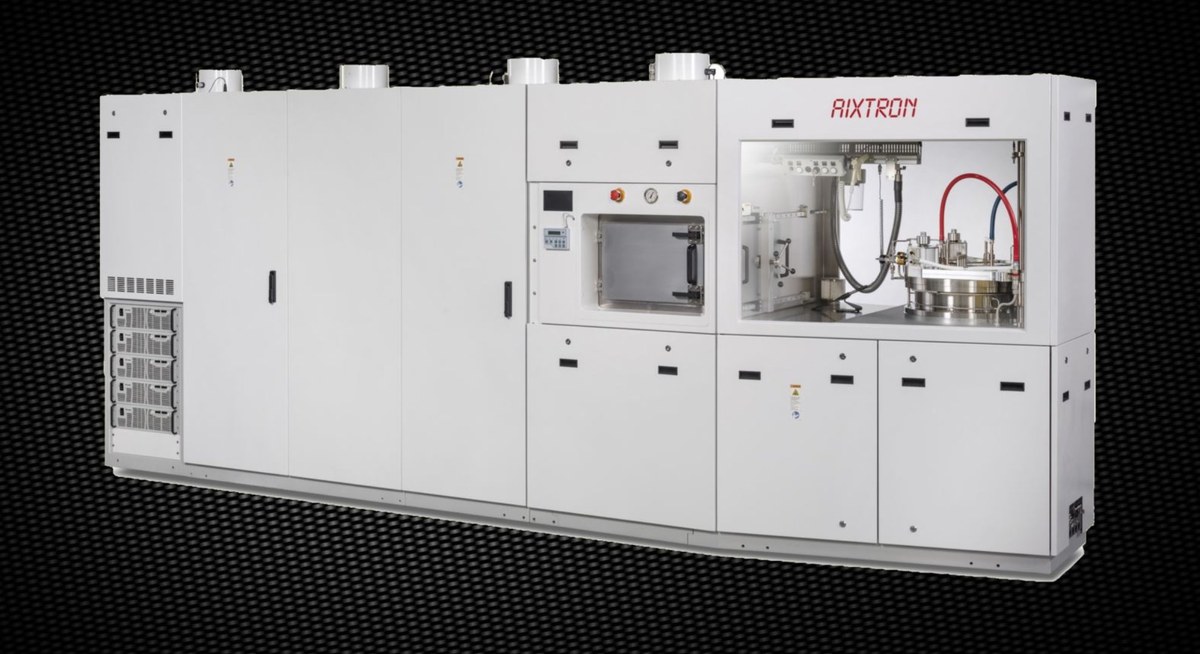
K1 MOCVD system technology for 2D materials
AIXTRON is the global market leader in the field of MOCVD system technology for the production of epitaxial layers for electronics and optoelectronics. AIXTRON has a broad background in metal organic vapor phase deposition (MOVPE) of III-V compound semiconductors for electronic and optoelectronic devices. Significant preliminary work in the field of 2D materials has already been carried out in other funded projects and as part of the company's internal research and development. The figure shows a prototype system which AIXTRON is using to investigate the deposition of 2D materials.
Today, 2D materials are mostly deposited in simple CVD systems. The equipment technology is based on experimental self-built systems and does not meet industrial requirements. Deposition using gaseous sources such as H2S, H2Se or organometallic sources is not very common. The requirements for the use of these source materials are high and cannot be reliably met by home-built equipment. From commercial CVD equipment manufacturers there are only few equipment concepts for the production of these special equipment for 2D materials. However, the outstanding and special properties of the 2D materials now require the professional and reproducible deposition of these layers in industrially suitable and highly scalable systems.
Goals for AIXTRON in the NEUROTEC II project are: |
|---|
|
|
|
|


